201 - Particle Detector Edit Page
Contents
- What is the Detector for Particle Physics Experiment?
- Classification of detectors by signals:
- Classification of detectors by measurement purposes:
- Silicon Carbide
What is the Detector for Particle Physics Experiment?
Detectors widely used in particle physics experiments extract signals in the
form of either photons or electrical current when particles pass through the detector material.
In addition, precise timing resolution is demanded especially for experiments in modern era
which is the characteristic different from others, for example, some of key detectors
used in astrophysics having long timing gate, human eyes etc.
Capability of reproducing the event topology by means of hit position information
is also commonly required for the particle detectors.
Those detectors are classifiable from several perspective, and the following examples are some of the typical classification.
Classification of detectors by signals:
1a) Producing photons as signal
- Cherenkov detectors (RICH, …)
- Counters (TOF, …)
1b) Producing electrical current as signal
- Silicon detectors (pixel/microstrip, …)
- Wire chambers (MWDC, …), TPC
- …
Classification of detectors by measurement purposes:
2a) Measurement of particle Momentum
- Silicon strip detectors
- Drift chambers
2b) Measurement of particle Vertex
- Silicon pixel detectors
2c) Measurement of particle Energy
- Calorimeters (ECal/HCal)
2d) Measurement of particle ID
- Drift chambers
- TOFs
- RICH
- …
**Above list/format is a first template (March 6th, 2021).
Silicon Carbide
3a)Crystal structure of silicon carbide
One of the differences between silicon carbide and silicon: silicon carbide has a polycrystalline crystal structure, such as 3C, 4H, 6H.

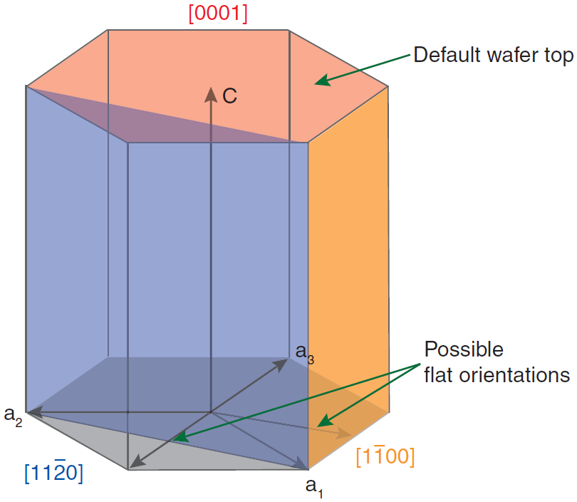
In hexagonal crystal structures, four Miller indices (a1, a2, a3, c) are commonly used to indicate directions.
However, it can be proved that there are the following relations between a1, a2 and a3: a1 + a2 + a3 = 0.
Therefore, it is simple and efficient to use only three Miller indices (a1, a2, and c) to indicate the direction, regardless of a3.
For example, the direction [11(-2)0] is simplified as as {1 1 0}.
3b) Layer structure of SiC
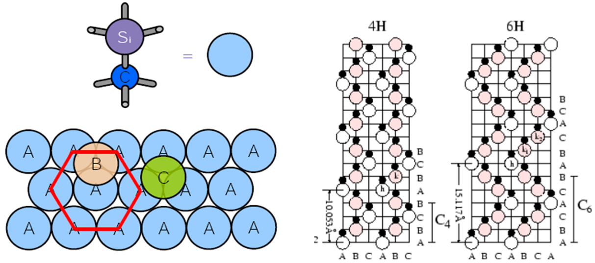
Both 4H-SiC and 6H-SiC lattices belong to hexagonal lattice structure, and the difference lies in the sequence of accumulation layers.For 4H-SiC, the deposit order is ABCB and for 6H-SiC, the deposit order is ABCACB.as shown in Figure 2.

The direction of accumulation along the upward direction is the C-axis in the previous image, i.e. [0001] direction.
3c) Miscut angle
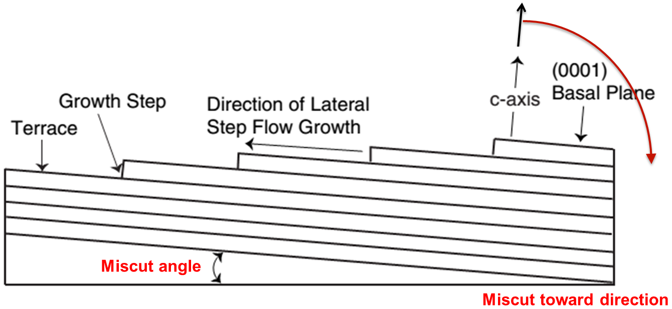
In the process of silicon carbide wafer production, the crystal growth is not completely along the normal direction of the wafer surface, but there is an angle between the growth direction and the normal direction of the wafer surface.This Angle can be called a miscut Angle. The miscut angle is usually in the range of 3.5 - 8.5°.

##Reference
[1] Synopsys.TCAD Sentaurus™ Tutorial.Sentaurus Device.v2018.
[2] Synopsys.Sentaurus™ Device User Guide.June 2018.