205 - Timing Detector Edit Page
Contents
- What is Timing Detector ?
- Time resolution of 3D semiconductor
- The time resolution simulation of silicon detector
What is Timing Detector ?
Time resolution of 3D semiconductor

The time resolution of a detector is largely given by jitter contribution and time walk contribution.
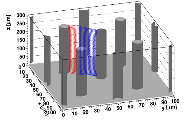
1.Noise can cause the fluctuation of threshold time, which is the main contribution of timing jitter. The noise is determined by the ratio of the rise time of the signal waveform and signal to noise ratio. Due to the detector cell of 3D detector is only about 30 \(\mu\) m, the rise time is small. When the signal to noise ratio is small, the jitter contribution to time resolution is relatively more important and possibly even dominant. When the signal to noise is enough (like Low Gain Avalanche Detectors (LGAD)), the jitter contribution can be ignored.
2.The time work contribution is caused by the difference in signal height and signal shapes.
- The difference in signal height can be reduced by using Constant Fraction Discrimination(CFD).
- The signal shapes are mainly affected by the differences in drift paths of generated carriers. Fluctuations in ionization rates along the track path (Landau fluctuations) add to the differences in pulse shapes. In 3D detectors, Landau fluctuations are less important because of charges generated at different depths have the same drift distance to the collection electrode. The time walk contribution mainly depends on the location of the mpact within the cell of the detector. [1]
The conclusion is that the time walk contribution for time resolution of 3D semiconductor detector is mainly given by the location of impact within the detector.
The time resolution simulation of silicon detector
The time resolution simulation of the silicon detector is essential for designing and improving the timing detector, and the simulation can predict the operation of the silicon detector to a certain extent. The simulation comprises four parts: electric and weighting field calculation, the charge generation by incident particles, the drift of the generated charge and the calculation of induced current, and the readout electronics.
1. Electric and Weighting Field Calculation
The electric potential \(V_{E}\) at the point “A” in a static electric field E is given by:
\[V_{E}=-\int_{C}Edl \tag{1-1} \label{eq1}\]where C is the path connecting the “A” point with zero potential. According to Gauss’s law and Poisson’s equation, the electric potential satisfies:
\[-\nabla^{2}V_{E} = \rho/\varepsilon_{0} \tag{1-2} \label{eq2}\]where \(\rho\) is the total charge density, and \(\varepsilon_{0}\) is permittivity of vacuum. if the material of detector is silicon and the effective concentration of the detector is \(N_{eff}(\vec{r})\). The equation becomes [2]:
\[-\nabla^{2}V_{E}(\vec{r}) = \frac{e_{0}N_{eff}(\vec{r})}{\varepsilon_{S_{i}}\varepsilon_{0}} \tag{1-3} \label{eq3}\] \[E(\vec{r})=-\nabla V_{E}(\vec{r}) \tag{1-4} \label{eq4}\]At the borders of simulated volume, the first derivative of the electric potential is 0. The boundary conditions were [2]:
\[\frac{\partial V_{E}}{\partial x}=0,\frac{\partial V_{E}}{\partial y}=0,\frac{\partial V_{E}}{\partial z}=0 \tag{1-5} \label{eq5}\]The \(V_{E}\) is equal to the applied voltage at the electrodes, and the \(V_{E}\) is 0 at the readout electrodes. By solving equations \(\eqref{eq3}\), \(\eqref{eq4}\) and \(\eqref{eq5}\), we can get the electric field distribution of the detector.
The weighting potential \(U_{w}(\vec{r})\) is the ratio of the potential of “A” point and after one or more potentials and charges are changed. The weighting field \(E_{w}(\vec{r})=-\nabla U_{w}(\vec{r})\) is a measure of electrostatic coupling between the point “A” and the detector electrode after one or more potentials and charges are changed.
The \(E_{w}(\vec{r})\) and \(U_{w}(\vec{r})\) are obtained as a solution of the equation \(\eqref{eq3}\) with the following boundary conditions [2]:
- \(U_{w}(\vec{r})=1\) at the readout electrode, \(U_{w}(\vec{r})=0\) at the other electrodes.
- \[\frac{\partial U_{w}(\vec{r})}{\partial x}=0,\frac{\partial U_{w}(\vec{r})}{\partial y}=0,\frac{\partial U_{w}(\vec{r})}{\partial z}=0 \tag{1-6} \label{eq6}\]
The calculation of the electric and weighting field is important for the simulation of carrier drift.
2. Charge generation by incident particles
When a Minimum Ionizing Particle (MIP) particle through the detector, the energy loss of the particle in silicon is:
\[\Delta E_{S{i}} = \frac{dE}{dx}\Delta x \tag{2-1} \label{eq7}\]where the most probable energy loss \(\frac{dE}{dx}\) in silicon is 273 eV/\(\mu\)m, and the \(\Delta x\) is the drift distance of the particle.
If we divide the track of particle into N steps, the amount of charge generated in i-th step is:
\[Q_{i}=\frac{1}{3.6eV}(\frac{dE}{dx})_{i} \Delta x_{i} \tag{2-1} \label{eq8}\]Through \(\eqref{eq8}\), we can roughly estimate that there will be about 7500 electron-hole pairs generated when a MIP particle pass through the sensor with a thickness of 100\(\mu\)m.
Reference
[1]. G. Kramberger et al. Timing performance of small cell 3D silicon detectors. DOI: 10.1016/j.nima.2019.04.088
[2]. G. Kramberger et al. Signal development in irradiated silicon detectors. CERN-THESIS-2001-038