JadePix Edit Page
Contents
- Test beam measurements of an irradiated prototype pixel sensor designed for the CEPC vertex detector
- Characterization of the first prototype CMOS pixel sensor developed for the CEPC vertex detector
Test beam measurements of an irradiated prototype pixel sensor designed for the CEPC vertex detector
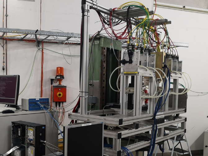
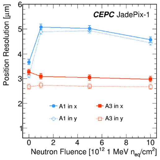
The Circular Electron Positron Collider (CEPC) has been proposed as a Higgs factory to measure the properties of the Higgs boson with unprecedented precision and to guide the searches for new physics. To meet the stringent physics requirements, it is necessary to design and construct its vertex detector with the state-of-theart silicon detector technologies. The first prototype CMOS pixel sensor, named JadePix-1, was developed for the CEPC vertex detector and its performance was already characterized with radioactive sources in laboratory. This prototype sensor was further characterized at the DESY test beam facility. Results are reported on charge collection, cluster size, position resolution and detection efficiency before and after the sensor samples exposed to neutron irradiation up to the fluence level of \(10^{13}\) 1 MeV \(n_{eq}∕cm^2\).
Further reading: Y. Han, et al., Test beam measurements of an irradiated prototype pixel sensor designed for the CEPC vertex detector, Nucl. Instrum. Methods A 977 (2020) 163267
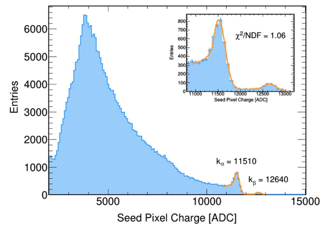
Characterization of the first prototype CMOS pixel sensor developed for the CEPC vertex detector
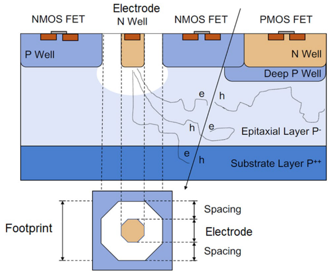
Purpose CMOS pixel sensor has become extremely attractive for future high-performance tracking devices. It has been proposed for the vertex detector at the Circular Electron Positron Collider, which will allow precision measurements of the properties of the Higgs boson. To meet the stringent requirements for low power consumption, it is necessary to optimize the pixel sensor diode geometry to reach a high charge-over-capacitance ratio that allows reduction in analog power consumption.
Methods Collection electrode size and footprint are two critical elements in sensor diode geometry and have deciding impacts on the charge collection performance. A prototype CMOS pixel sensor, named JadePix-1, has been developed with pixel sectors implemented with different electrode sizes and footprints, and its charge collection performance has been characterized with radioactive sources.
Results Charge-to-voltage conversion gains for pixel sectors under test have been calibrated with low-energy X-rays. Characterization results have been obtained for equivalent noise charge (below 10e−), charge collection efficiency (around 40%), charge-over-capacitance ratio (above 0.015 V) and signal-to-noise ratio (higher than 55).
Conclusion Small collection electrode size and large footprint are preferred to achieve high charge-over-capacitance ratio that promises low analog power consumption. Ongoing studies on sensor performance before and after irradiation, combined with this work, will conclude the diode geometry optimization.
Further reading: L.J. Chen, et al., Characterization of the first prototype CMOS pixel sensor developed for the CEPC vertex detector, Radiation Detection technology and Methods 3:45 (2019)