https://doi.org/10.1002/pssa.201300233
In this paper, a new versatile scheme to simulate DLTS signals was presented which allows an efficient but still flexible implementation and evaluation of physical processes that govern the coupling of the defect levels to the respective carrier bands. This can play a key role in understanding the electrical properties of extended defects.
Simulation reproduces some below effects:
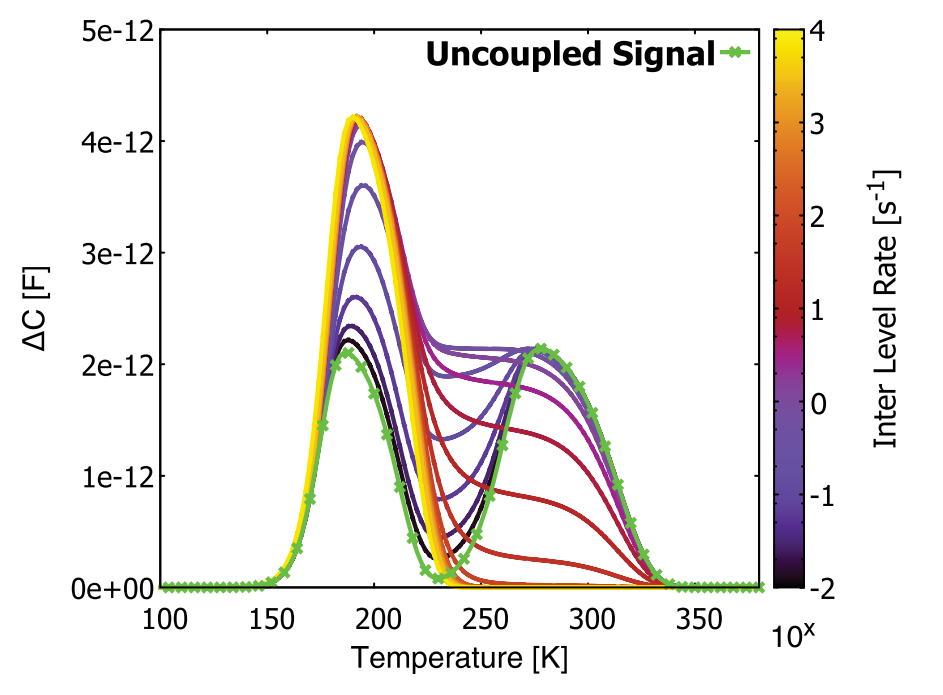
- Coupling of defect levels: Due to the spatial proximity of the bound impurities to the dislocation loop interactions between the defects should not be neglected.The results are shown in figure. High coupling strength leads to the absorption of the DLTS peak which is normally seen at higher temperatures and a broadening of the absorbing peak with simultaneous increase of its amplitude is observed.In the same way, the broadening of a defect level distribution in the band gap causes a broadening of the measured DLTS signal.
- Impact of Coulomb energy on DLTS signal: The “Coulomb ladder” of energy levels results in a shift of the peak to lower temperatures similar to the case of distributed defect levels E_{T,i}.
